NASA Technical Reports Server (Ntrs) 19990062250: Chemical Sensors Based on Ir Spectroscopy and Surface-Modified waveguides by NASA Technical Reports Server (Ntrs); published by
NASA Technical Reports Server (Ntrs) 19990062250: Chemical Sensors Based on Ir Spectroscopy and Surface-Modified waveguides by NASA Technical Reports Server (Ntrs); published by
We report a waveguide crossing based on a multimode-interference (MMI) structure for metal-insulator-metal (MIM) waveguides. The MMI-based crossing comprises two orthogonal intersecting MMI waveguides that are con...
详细信息
We report a waveguide crossing based on a multimode-interference (MMI) structure for metal-insulator-metal (MIM) waveguides. The MMI-based crossing comprises two orthogonal intersecting MMI waveguides that are connected to the single-mode input/output waveguide symmetrically. Single self-images are formed at the cross- ing center and output plane of the MMI waveguide, thereby mitigating the crosstalk and improving the through- put. The characteristics of the proposed MMI-based crossing are investigated with the finite element method of Comsol Multiphysics. The results show that the throughput reaches -1.8 dB and the crosstalk is less than -46 dB at the wavelength of 1550 nm.
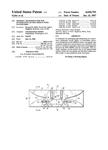
NASA Technical Reports Server (Ntrs) 20080008223: General Technique for the Integration of Mic/Mmic's with waveguides by NASA Technical Reports Server (Ntrs); published by
NASA Technical Reports Server (Ntrs) 20080008223: General Technique for the Integration of Mic/Mmic's with waveguides by NASA Technical Reports Server (Ntrs); published by
NASA Technical Reports Server (Ntrs) 20020027138: Coupling Between Finite Ground Coplanar waveguides Embedded in Polyimide Layers for 3D-Mmics on Si by NASA Technical Reports Server (Ntrs); published by
NASA Technical Reports Server (Ntrs) 20020027138: Coupling Between Finite Ground Coplanar waveguides Embedded in Polyimide Layers for 3D-Mmics on Si by NASA Technical Reports Server (Ntrs); published by
NASA Technical Reports Server (Ntrs) 20020038951: Electromagnetic Modeling of Distributed-Source-Excitation of Coplanar waveguides: Applications to Traveling-Wave Photomixers by NASA Technical Reports Server (Ntrs); p...
详细信息
NASA Technical Reports Server (Ntrs) 20020038951: Electromagnetic Modeling of Distributed-Source-Excitation of Coplanar waveguides: Applications to Traveling-Wave Photomixers by NASA Technical Reports Server (Ntrs); published by
NASA Technical Reports Server (Ntrs) 20110023771: Arrays of Carbon Nanotubes as Rf Filters in waveguides by NASA Technical Reports Server (Ntrs); published by
NASA Technical Reports Server (Ntrs) 20110023771: Arrays of Carbon Nanotubes as Rf Filters in waveguides by NASA Technical Reports Server (Ntrs); published by
Series expansions of unknown fields phi = Sigma phi(n)Z(n) in elongated waveguides are commonly used in acoustics, optics, geophysics, water waves and other applications, in the context of coupled-mode theories (CMTs)...
详细信息
Series expansions of unknown fields phi = Sigma phi(n)Z(n) in elongated waveguides are commonly used in acoustics, optics, geophysics, water waves and other applications, in the context of coupled-mode theories (CMTs). The transverse functions Z(n) are determined by solving local Sturm-Liouville problems (reference waveguides). In most cases, the boundary conditions assigned to Z(n) cannot be compatible with the physical boundary conditions of phi, leading to slowly convergent series, and rendering CMTs mildslope approximations. In the present paper, the heuristic approach introduced in Athanassoulis & Belibassakis (Athanassoulis & Belibassakis 1999 J. Fluid Mech. 389, 275-301) is generalized and justified. It is proved that an appropriately enhanced series expansion becomes an exact, rapidly convergent representation of the field phi, valid for any smooth, non-planar boundaries and any smooth enough phi. This series expansion can be differentiated termwise everywhere in the domain, including the boundaries, implementing an exact semi-separation of variables for non-separable domains. The efficiency of the method is illustrated by solving a boundary value problem for the Laplace equation, and computing the corresponding Dirichlet-to-Neumann operator, involved in Hamiltonian equations for nonlinear water waves. The present method provides accurate results with only a few modes for quite general domains. Extensions to general waveguides are also discussed.
Good sensing performance is observed in metal-dielectric-metal (MDM) waveguides in recent research. However, Ag will be oxidized in air. The oxidization layer makes the sensing performance not as high as before. Plati...
详细信息
Good sensing performance is observed in metal-dielectric-metal (MDM) waveguides in recent research. However, Ag will be oxidized in air. The oxidization layer makes the sensing performance not as high as before. Plating an SiO2 film on the surface of the Ag waveguide not only can avoid oxidization but can keep good sensing performance through our numerical discussion as well. The decaying rate of electric field E at the interface and inside is also defined to illustrate the phenomenon mentioned above. We hope our findings will provide guidance for the integrated plasmonic devices.
We demonstrate a steplike optical modulation based on the activation and deactivation of a bistable localized structure using a photoinduced and reconfigurable miniaturized 30×30 μm electroactivated funnel wave...
详细信息
We demonstrate a steplike optical modulation based on the activation and deactivation of a bistable localized structure using a photoinduced and reconfigurable miniaturized 30×30 μm electroactivated funnel waveguide. Control of a single 10−μm-diameter spot in a 200−μm-diameter vertical-cavity surface-emitting laser at 980 nm is achieved modulating the phase of an exciting beam in the specific position of the spot in the cavity. This localized on-off response can be scaled into arrays and offer a possible route to fast integrated optical logical functions and memory at low intensities at near-infrared wavelengths.
As modern complementary-metal-oxide-semiconductor (CMOS) circuitry rapidly approaches fundamental speed and bandwidth limitations, optical platforms have become promising candidates to circumvent these limits and faci...
详细信息
As modern complementary-metal-oxide-semiconductor (CMOS) circuitry rapidly approaches fundamental speed and bandwidth limitations, optical platforms have become promising candidates to circumvent these limits and facilitate massive increases in computational power. To compete with high density CMOS circuitry, optical technology within the plasmonic regime is desirable, because of the sub-diffraction limited confinement of electromagnetic energy, large optical bandwidth, and ultrafast processing capabilities. As such, nanoplasmonic waveguides act as nanoscale conduits for optical signals, thereby forming the backbone of such a platform. In recent years, significant research interest has developed to uncover the fundamental physics governing phenomena occurring within nanoplasmonic waveguides, and to implement unique optical devices. In doing so, a wide variety of material properties have been exploited. CMOS-compatible materials facilitate passive plasmonic routing devices for directing the confined radiation. Magnetic materials facilitate time-reversal symmetry breaking, aiding in the development of nonreciprocal isolators or modulators. Additionally, strong confinement and enhancement of electric fields within such waveguides require the use of materials with high nonlinear coefficients to achieve increased nonlinear optical phenomenon in a nanoscale footprint. Furthermore, this enhancement and confinement of the fields facilitate the study of strong-field effects within the solid-state environment of the waveguide. Here, we review current stateof- the-art physics and applications of nanoplasmonic waveguides pertaining to passive, magnetoplasmonic, nonlinear, and strong-field devices. Such components are essential elements in integrated optical circuitry, and each fulfill specific roles in truly developing a chip-scale plasmonic computing architecture.


暂无评论